
Bottom-Up Assembly of Structures on a Substrate
ID# 2007-3401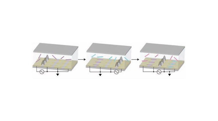
Technology Summary
Photolithography continues to be the dominant technology in the fabrication of electronic devices today. However, the process has drawbacks, including the ability to only process one material at a time and ever-increasing challenges to pattern at smaller scales. The emergence of nanomaterials and nanostructures, such as nanowire, nanoparticles, etc., as a viable technology that can overcome the limitations of photolithography depends on finding processes that can accurately place and position such nanostructures so that electronic devices can be fabricated.
This invention describes a programmed direct assembly method for positioning and integrating different populations of micro/nano structures on a substrate. The nanostructures can be synthesized under optimal conditions off of the substrate prior to their assembly on the substrate and then dispersed in delivery medium and accurately placed and positioned on the substrate. Electric-field forces are also used with programmed control for nanostructure placement.
Application & Market Utility
A variety of materials may be used allowing for the creation of heterogeneous devices. Further, the nanostructures can be chemically functionalized prior to placement to allow for the creation of devices or arrays of devices that have the ability to selective detect analytes. This invention provides the means to accurately and reliably engineer and manufacture devices based on micro/nano structures possessing a broad set of applications for electrical devices and sensors, including biological/chemical sensors with electrical, as opposed to optical, outputs.
Next Steps
Prototype nanoscale devices have been manufactured using this process. Protected by U.S. Patent 8,361,297. Seeking licensing opportunities.