
Method of Growing Crystalline Layers on Amorphous Substrates
ID# 2018-4743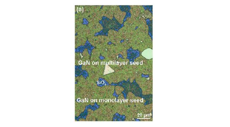
Technology Summary
Methods of producing Group-III chalcogenide (GIIIC) seed layers have been developed, allowing for an ultra-thin nanocrystalline Group III nitride layer to form on amorphous substrates such as silicon or silicon dioxide. Effectively, the GIIIC materials are used as a precursor to group III-V semiconductors by growing the GIIIC materials on a substrate and subsequently treating the material with nitridation and/or exfoliation in order to produce a semiconductor with a band gap of about 1-3 eV.
Application & Market Utility
Chalcogenide semiconductors are important materials for optical applications such as solar cells, thermal imaging, sensors and electrical applications such as LEDS and electrical devices. The present invention is a thin film that acts as a precursor to such semiconductors. This invention provides a more reliable and cost-effective method of synthesizing Group III-V semiconductors. Further, this invention enables high quality GaN synthesis on amorphous substrates such as silica and glass, thereby expanding the functionality of nitride materials and the library of possible growth substrates.
Next Steps
Seeking research collaboration and licensing opportunities.