
Two Dimensional Electrostrictive Field Effect Transistor
ID# 2017-4577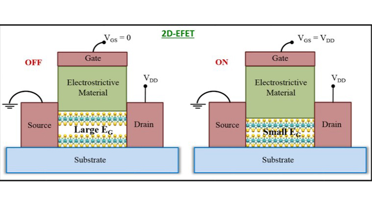
Technology Summary
This two-dimensional electrostrictive field effect transistor (2D-EFET) meets the low power and high-performance criterion for post-CMOS computing and concurrently enables aggressive channel length scaling. Its ultra-thin body and electrostatic integrity enables scaling beyond 10 nm technology node using the principle of voltage induced strain transduction. The device employs electrostrictive or piezoelectric or ferroelectric material as a gate oxide, which expands in response to an applied gate bias and thereby transduces an out-of-plane stress on the 2D channel material. This stress reduces the inter-layer distance between the consecutive layers of the semiconducting 2D material and dynamically reduces its bandgap to zero i.e., converts it into a semi-metal. This 2D-EFET offers a steep subthreshold swing below 60 mV/decade and provides significantly higher ON-state current density.
Application & Market Utility
Scaling has driven the success of metal oxide semiconductor field effect transistors (MOSFETs). However, limitations in dimensional scaling and voltage scaling ensure that the era of complementary metal oxide semiconductor (CMOS) will plateau. Research on post-Si-CMOS devices face two key challenges: length scaling and voltage scaling. Post-CMOS device design require that the subthreshold swing (SS) slope should be as abrupt as possible (ideally zero) to meet the low power requirement whereas the ON current should be as high as possible to increase the device’s speed.
Next Steps
2D-EFET transistor would serve as a disruptive platform that would require re-engineering of the bigger unit that uses the transistor as a component.