
Vertical 2D Fins for Advanced Electronics and Optoelectronics
ID# 2015-4374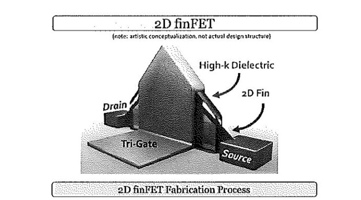
Technology Summary
A novel method to overcome poor device design in 2D materials by forming isolated vertical fins rather than lateral fins. The method can also control for dense crowding of the vertical structures, which would lead to unusable material. The method allows for fabrication of vertical homogenous and heterogenous two-dimensional structures perpendicular to planar structures, which are free-standing and electrically isolated. The substrates may comprise crystalline, polycrystalline or amorphous structures, such as SiC, sapphire, SiO2, graphene, graphite, poly-Si, poly-SiC and similar materials. The fabricated vertical 2D structures having a thickness < 20 layers. The researchers have also shown multilayered structures having layer thickness of less than 1nm thickness. Results have been confirmed using TEM and SEM images.
Application & Market Utility
The disclosed invention seeks to subvert the semiconductor industry’s reliance upon silicon in traditional “FinFETS”. Until now, 2-dimensional materials and device designs have not been able to outperform these traditional semiconductors because below 30 nm on traditional planar FETs requires extreme fabrication techniques. Applications: 2D “fin” field effect transistors, other semiconductors, catalysis, photovoltaics. The vertical 2D structures are also suitable for coatings including but not limited to conductive, insulating and protective layers.
Next Steps
Seeking research collaboration and licensing opportunities.